Welcome to Our Company

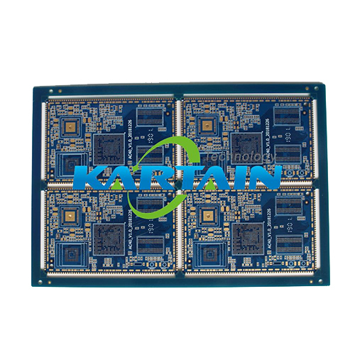
12L HDI PCB
Product Details:
- Insulation Resistance 10
- Silkscreen White
- Min. Line Spacing 0.076 mm (3 mil)
- Board Type Rigid
- Voltage Endurance 1500 V
- Soldermask Green LPI
- Impedance 10% Controlled Impedance
- Click to View more
X
12L HDI PCB Price And Quantity
- 100 Unit
- 0.025 mm
- Available
- 7-12 Days
- Laser Drilled Microvias
- 0.7%
- Rolled/Annealed for Inner Layers
- 0.01 mm
- 10:1
- >170C
- 130C
- 0.03-0.05 m Au over 3-6 m Ni
12L HDI PCB Product Specifications
- HDI
- Rigid
- 1500 V
- Green LPI
- HDI PCB
- White
- 1.6 mm
- 10
- 12
- 0.076 mm (3 mil)
- 600 mm x 400 mm
- SMD, Through-Hole Compatible
- Flying Probe, E-test
- No
- 0.076 mm (3 mil)
- UL94-V0
- 0.1 mm (Min.)
- 10% Controlled Impedance
- Yes
- ENIG (Electroless Nickel Immersion Gold)
- Green
- 1 Oz
- 0.025 mm
- Available
- 7-12 Days
- Laser Drilled Microvias
- 0.7%
- Rolled/Annealed for Inner Layers
- 0.01 mm
- 10:1
- >170C
- 130C
- 0.03-0.05 m Au over 3-6 m Ni
12L HDI PCB Trade Information
- Cash in Advance (CID)
- 5000 Unit Per Month
- 2-5 Days
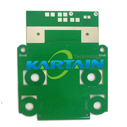
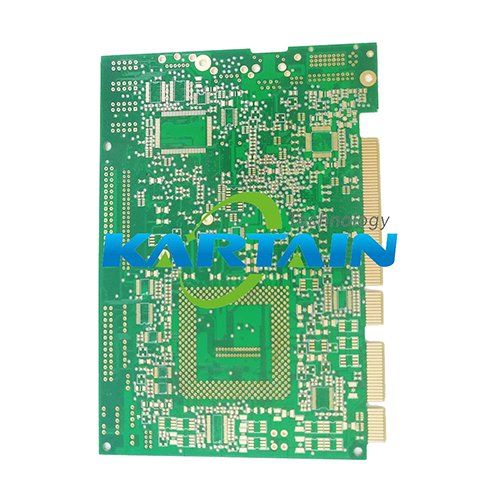
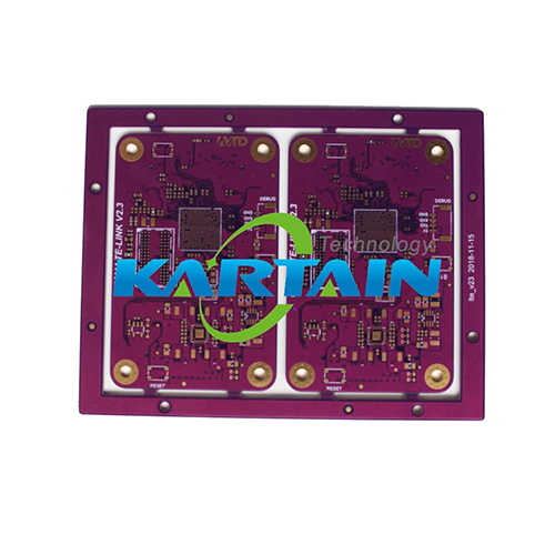
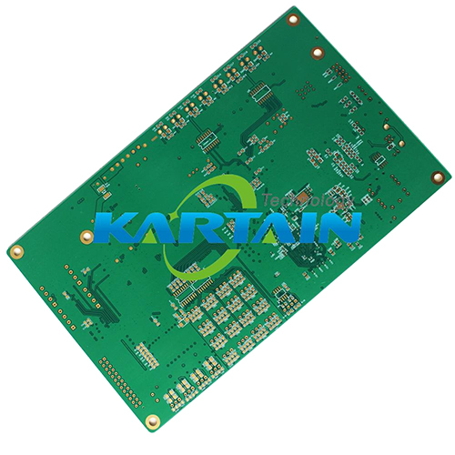
Product Description
Select this 12L HDI PCB for your next project and experience unrivaled performance where only the finest components deliver. Crafted with laser-drilled microvias and a dominant aspect ratio of 10: 1, this PCB offers striking dependability with a Glass Transition Temperature exceeding 170C. With a majestic finish of 0.03-0.05 m Au over 3-6 m Ni and an incredibly tight via tolerance of 0.025 mm, this scarce solution is highly sought-after for precision-critical applications. Pick yours now to benefit from OEM/ODM services, 7-12 days production lead time, and superior quality fit for leading-edge innovation.
Key Features and Applications of 12L HDI PCB
Engineered with outstanding details, this 12-layer rigid HDI PCB is suitable for high-reliability sectors including telecom, medical equipment, and automotive electronics. Its laser-drilled microvias ensure superior signal integrity, while its robust copper foil and advanced ENIG surface finish guarantee durability. The exceptional warpage control and flatness make it an ideal pick for high-density SMD and through-hole assemblies. As a select, high-tech choice, it excels in scenarios demanding the utmost electrical and mechanical performance.
Certifications, Supply, and Order Processing Advantage
This 12L HDI PCB is certified to UL94-V0 flame resistance and tested for 10 insulation resistance and 1500 V voltage endurance. Samples are available by request for evaluation purposes. As a leading exporter, manufacturer, and supplier from China, we ensure rapid order processing and reliable global supply ability. Benefit from competitive sale prices and the lowest price guarantee on bulk orders, making advanced PCB technology more accessible for your business needs.
FAQs of 12L HDI PCB:
Q: How does the 12L HDI PCB maintain precise tolerance and signal integrity?
A: The 12L HDI PCB utilizes laser-drilled microvias and rolled/annealed copper foil, achieving via tolerance of 0.025 mm and superior flatness. This precise engineering ensures stable signal routing and minimizes defects in dense, multilayer designs.Q: What special features distinguish this PCB from standard multilayer boards?
A: This HDI PCB features a 10: 1 aspect ratio, ENIG finish, and advanced warpage control (0.7%%), supporting both SMD and through-hole components. Its controlled impedance (10%%) and superior insulation resistance suit demanding high-frequency and reliability applications.Q: When can I expect the production and delivery of my PCB orders?
A: Production lead time is typically 7-12 days. Delivery schedules depend on order volume and shipping arrangements, with expedited options available for urgent requirements.Q: Where can this PCB be effectively applied?
A: This PCB is ideal for advanced electronics such as telecommunication devices, medical instruments, automotive systems, and industrial control units where high layer count and signal precision are critical.Q: What process is involved in ensuring product quality?
A: Each board is subject to rigorous Flying Probe and E-testing to guarantee electrical integrity and performance. The production process incorporates strict warpage and impedance control, certified by international standards like UL94-V0.Q: What are the main benefits of ordering this 12L HDI PCB?
A: Customers enjoy high performance, OEM/ODM customization, rapid turnaround, and comprehensive support. With competitive sale prices and warranty assurance, this PCB is a top choice for industries requiring reliability and innovation.Tell us about your requirement

Price:
Quantity
Select Unit
- 50
- 100
- 200
- 250
- 500
- 1000+
Additional detail
Mobile number
Email

Other Products in 'UDP Package PCB' category
Contact Us
- 2nd Road, Xinfa Industrial Xinqiao Shajing Town Baoan, Shenzhen - 518125, Guangdong, China
- Phone : 86-755-23328853
Kartain Technology Co., Ltd.
- Mr. Eason Xiang
- Mobile : +8615814406156
- Send Inquiry
Products

 Send Inquiry
Kartain Technology Co., Ltd.
All Rights Reserved.(Terms of Use)
Developed and Managed by Infocom Network Private Limited.
Developed and Managed by Infocom Network Private Limited.
