Welcome to Our Company

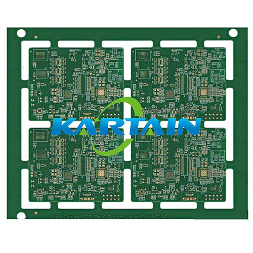
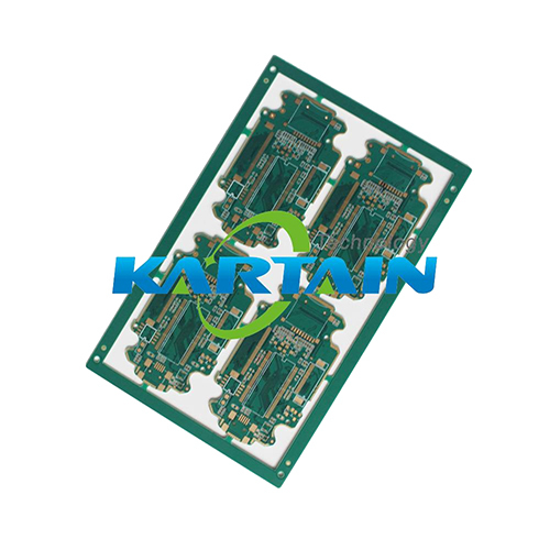
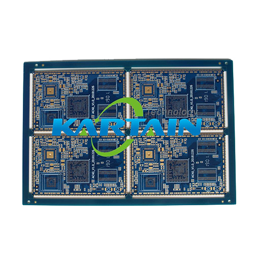
12layer HDI PCB
Product Details:
- Flame Resistance Level UL94 V-0
- Silkscreen White
- Min. Line Width 0.076mm (3mil)
- Insulation Resistance 10^12
- Test Flying Probe Test, E-Test
- Impedance Controlled (10%)
- Hole Size 0.2mm (min)
- Click to View more
X
12layer HDI PCB Price And Quantity
- 100 Unit
- 3+N+3
- Gerber/ODB++ Supported
- 0.05mm
- 510mm x 400mm
- Yes
- 0.1mm
- 1.0W/mK (for aluminum base)
- LPI (Liquid Photoimageable Ink)
- Immersion Gold
- Ni 2.5-5m / Au 0.03-0.08m
- 10:1
- Yes (Blind via/ Buried via/ Micro via)
- 0.75:1
- IPC-6012 Class 2/Class 3
- 3oz (inner/outer layers customizable)
- High-Density Interconnect, Communication Equipment, Automotive, Industrial Control
- 0.15mm
- 0.3mm
- 10m
12layer HDI PCB Product Specifications
- No
- 1.6mm
- 1500V (AC)
- Rigid
- Green
- No
- 0.076mm (3mil)
- Alumunium
- ENIG (Electroless Nickel Immersion Gold)
- 470mm x 320mm
- 12
- 1oz
- UL94 V-0
- White
- Yes
- Controlled (10%)
- 0.2mm (min)
- 10^12
- 0.076mm (3mil)
- Green
- PCB
- Flying Probe Test, E-Test
- 3+N+3
- Gerber/ODB++ Supported
- 0.05mm
- 510mm x 400mm
- Yes
- 0.1mm
- 1.0W/mK (for aluminum base)
- LPI (Liquid Photoimageable Ink)
- Immersion Gold
- Ni 2.5-5m / Au 0.03-0.08m
- 10:1
- Yes (Blind via/ Buried via/ Micro via)
- 0.75:1
- IPC-6012 Class 2/Class 3
- 3oz (inner/outer layers customizable)
- High-Density Interconnect, Communication Equipment, Automotive, Industrial Control
- 0.15mm
- 0.3mm
- 10m
12layer HDI PCB Trade Information
- Cash in Advance (CID)
- 5000 Unit Per Month
- 2-5 Days
Product Description
Encounter the exquisite quality of our rare 12-layer HDI PCB, crafted to exceed demanding industry standards. Capitalise on our advanced 3+N+3 layer stackup, offering astonishing blind/buried/micro via capabilities for maximal design flexibility. With an outstanding 10: 1 aspect ratio and customizable copper weights up to 3oz, each board demonstrates remarkable efficiency. Exceptional surface flatness (10m) and ENIG finish deliver reliability in critical applications. Buy directly from a remarked China-based manufacturer, ensuring RoHS compliance, IPC-6012 certification, and full design supportthis premium solution is scarce, so secure yours today.
Comprehensive Usage and Applications for 12-Layer HDI PCB
The 12-layer HDI PCB is engineered for versatility in numerous application areas, from high-density interconnect systems to automotive electronics, communication equipment, and industrial control. This board excels in both specific and general use scenarios, offering rigid design and advanced microvia technology. Ideal for prototypes and end-product integration, it handles demanding environments where precision and reliability are paramount. Design engineers can use Gerber or ODB++ files for seamless project execution, ensuring rapid development cycles in complex assemblies.
Premium Delivery, Sample Policy, and Payment Terms for HDI PCBs
We offer premium delivery of your 12-layer HDI PCBs, ensuring your order is shipped swiftly and securely. Competitive sample policies let you evaluate our products performance before large-scale procurement. Flexible payment terms accommodate your business needs, making the purchase process convenient. Our samples and bulk orders are processed promptly for timely delivery, ensuring clients receive a remarkable offer every time. Experience excellence from initial inquiry to final shipment, supported by dedicated service and warranty protection.
FAQs of 12layer HDI PCB:
Q: How can I use the 12-layer HDI PCB in my industrial or automotive projects?
A: The 12-layer HDI PCB is designed for advanced interconnect applications, making it ideal for industrial control systems and automotive electronics. Its robust layer stack and blind/buried via options facilitate compact, high-density designs for reliable performance in demanding environments.Q: What remarkable features distinguish this HDI PCB from standard multilayer boards?
A: Key distinguishing features include its 3+N+3 layer stackup, support for microvias, high aspect ratio (10: 1), thick customizable copper layers, controlled impedance, ENIG surface finish, and compliance with IPC-6012 Class 2/3, all of which ensure superior electrical and mechanical performance.Q: Where is this product manufactured and exported from?
A: This 12-layer HDI PCB is manufactured in China and can be exported worldwide. Our facility adheres to international quality standards, optimizing production for global supply.Q: What is the process for ordering and receiving samples of the PCB?
A: Simply contact us with your requirements and design files (Gerber or ODB++). We offer samples to test the boards excellence before moving to bulk orders. Samples and orders are shipped promptly with comprehensive support.Q: What benefits does the ENIG surface finish provide to the 12-layer HDI PCB?
A: ENIG (Electroless Nickel Immersion Gold) offers excellent surface flatness, superior solderability, and reliable performance with fine-pitch components such as BGAs, making it suitable for high-density board designs.Q: When can I expect my HDI PCBs to be shipped after placing an order?
A: Typically, PCBs are shipped shortly after order confirmation and finalization of design specifications. Delivery timelines depend on order size and customization, but our team ensures timely dispatch for both samples and bulk production.Tell us about your requirement

Price:
Quantity
Select Unit
- 50
- 100
- 200
- 250
- 500
- 1000+
Additional detail
Mobile number
Email

Other Products in 'UDP Package PCB' category
Contact Us
- 2nd Road, Xinfa Industrial Xinqiao Shajing Town Baoan, Shenzhen - 518125, Guangdong, China
- Phone : 86-755-23328853
Kartain Technology Co., Ltd.
- Mr. Eason Xiang
- Mobile : +8615814406156
- Send Inquiry
Products

 Send Inquiry
 Call Me Free
Kartain Technology Co., Ltd.
All Rights Reserved.(Terms of Use)
Developed and Managed by Infocom Network Private Limited.
Developed and Managed by Infocom Network Private Limited.
