Welcome to Our Company

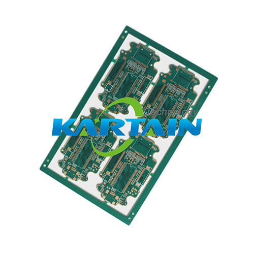
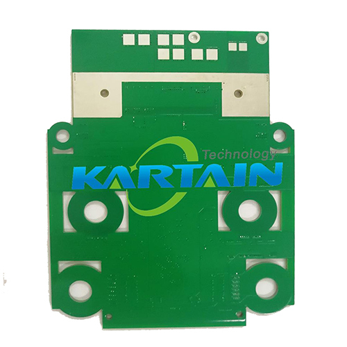
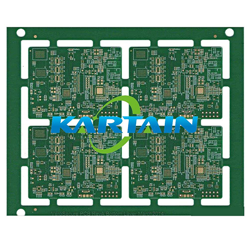
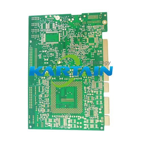
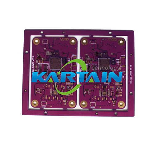
6Layers HDI PCB
Product Details:
- Hole Size 0.15 mm (Min.)
- Insulation Resistance >10
- Board Type Rigid
- Impedance 10% Controlled
- Test Flying Probe, AOI, E-test
- Soldermask Green
- Flame Resistance Level UL 94V-0
- Click to View more
X
6Layers HDI PCB Price And Quantity
- 100 Unit
- Supported
- 8:1
- 0.05 mm
- Yes
- Mobile Devices, High-Speed Communication, Industrial Control
- 130C
- Vacuum Sealed
- Green
- White
- 710 Days
- Yes
- 1-2-1 HDI Structure
6Layers HDI PCB Product Specifications
- Green
- No
- PCB
- Flying Probe, AOI, E-test
- ENIG (Electroless Nickel Immersion Gold)
- 10% Controlled
- Alumunium
- Green
- Yes
- Rigid
- >10
- 0.15 mm (Min.)
- 6 Layers
- White
- 1 oz
- 300 mm x 400 mm
- 1.6 mm
- 0.075 mm
- SMT/DIP Compatible
- 0.075 mm
- 2000V AC/min
- UL 94V-0
- Supported
- 8:1
- 0.05 mm
- Yes
- Mobile Devices, High-Speed Communication, Industrial Control
- 130C
- Vacuum Sealed
- Green
- White
- 710 Days
- Yes
- 1-2-1 HDI Structure
6Layers HDI PCB Trade Information
- Cash in Advance (CID)
- 5000 Unit Per Month
- 2-5 Days
Product Description
Experience the sublime sophistication of our Top 6Layers HDI PCB, expertly crafted for high-speed communications, mobile devices, and industrial control systems. With a decorated 1-2-1 HDI stack-up, this valiant rigid board supports both blind and buried vias and offers an impressive aspect ratio of 8: 1. Fresh green soldermask paired with white silkscreen ensures clear visibility and refined aesthetics. Manufactured with aluminum base materials, ENIG surface finish, and RoHS-compliance, this limited-time offering delivers exceptional electrical reliability and robust insulation resistance. Benefit from quick 710 day lead times, warranty support, and vacuum-sealed packagingperfect for critical export demands worldwide.
6Layers HDI PCB: Advantages and Key Applications
Engineered for precision, the 6Layers HDI PCB boasts sublime impedance control (10%%), minimized layer alignment tolerance (0.05 mm), and robust insulation resistance exceeding 10 . With valiant performance under voltages up to 2000V AC/min and a flame resistance of UL 94V-0, it stands as a top choice for demanding sectors like mobile electronics, high-speed communications, and industrial automation. Its versatile design supports SMT and DIP components, making it ideal for advanced device production and stringent industrial environments.
6Layers HDI PCB: Payment, Packaging, and Sampling Policy
For export markets, our 6Layers HDI PCB is vacuum-sealed to guarantee product integrity during worldwide dispatching. We offer quick dispatch times post confirmed payment, supporting major payment terms to ensure smooth transactions. Sample policies are designed for customer confidenceallowing evaluation prior to bulk orders. Each shipment is prepared for international standards, ensuring rapid delivery and secure transport, making us a decorated supplier trusted for reliability and seamless order handling across global markets.
FAQs of 6Layers HDI PCB:
Q: How does the 6Layers HDI PCB benefit high-speed communication applications?
A: The 6Layers HDI PCB offers excellent impedance tolerance (10%%), reliable signal integrity, and robust electrical characteristics, making it highly suitable for high-speed communication systems requiring consistent and stable performance.Q: What quality tests are performed on these HDI PCBs before dispatching?
A: Each PCB undergoes stringent evaluations including Flying Probe, Automated Optical Inspection (AOI), and E-tests. This ensures full compliance with electrical and physical specification standards before quick dispatch to customers.Q: Where can the 6Layers HDI PCB be effectively utilized?
A: These boards are ideal for sophisticated mobile devices, high-speed communication networks, and industrial control systems. Their structure accommodates both SMT and DIP components, enhancing device miniaturization and reliability.Q: What is the minimum production lead time and how are boards packaged for shipment?
A: Standard lead time is 710 days. PCBs are securely vacuum-sealed and packed according to export-grade protocols, ensuring safe and fresh delivery worldwide.Q: What payment terms and sample policies do you offer for international buyers?
A: We accommodate major international payment methods and provide sample PCBs for evaluation. This approach assures customers of product quality prior to confirming larger orders.Tell us about your requirement

Price:
Quantity
Select Unit
- 50
- 100
- 200
- 250
- 500
- 1000+
Additional detail
Mobile number
Email

Other Products in 'UDP Package PCB' category
Contact Us
- 2nd Road, Xinfa Industrial Xinqiao Shajing Town Baoan, Shenzhen - 518125, Guangdong, China
- Phone : 86-755-23328853
Kartain Technology Co., Ltd.
- Mr. Eason Xiang
- Mobile : +8615814406156
- Send Inquiry
Products

 Send Inquiry
 Call Me Free
Kartain Technology Co., Ltd.
All Rights Reserved.(Terms of Use)
Developed and Managed by Infocom Network Private Limited.
Developed and Managed by Infocom Network Private Limited.
